As the need for higher resolution and higher-speed signal chains increases for industrial equipment such as programmable logic controllers, weigh scales and automated test equipment, so does the need for high-precision amplifiers acting as analog-to-digital converter (ADC) drivers and voltage reference buffers in such signal chains.
In this article, I’ll discuss two common design challenges when designing a precision signal chain, and how to overcome them. But first, it’s important to understand chopper amplifiers, which are popular in these systems.
What is a chopper amplifier?
A chopper amplifier is a type of zero-drift operational amplifier (op amp) known for having a very low offset voltage, thanks to an internal topology that minimizes the amplifier’s offset regardless of configuration. This results in very low offset errors (offset, drift, common-mode rejection ratio [CMRR], power-supply rejection ratio [PSRR] and open-loop voltage gain [Aol]), as shown in Figure 1. Another benefit of this topology is that it has flat 1/f or flicker noise, since the amplifier perceives (and thus minimizes) low-frequency noise as a DC error. Chopper amplifiers are an excellent choice for applications requiring high precision across frequencies ranging from DC to tens of kilohertz, such as precision temperature monitoring, Wheatstone bridge measurements and voltage reference buffering.

Figure 1: Chopper amplifiers have low offset errors and a flat 1/f noise curve due to their architecture
Now, let’s get back to the challenges facing precision signal chains.
Challenge No. 1: minimizing offset errors across temperature
One of the biggest challenges when designing a precision signal chain is minimizing the offset errors introduced by the ADC driver and reference buffer. While performing calibration during production can improve offset, CMRR, PSRR and Aol performance, offset voltage drift is difficult and expensive to calibrate It requires changing the system temperature in production or adding a calibration loop, which increases system size and bill-of-materials count. Instead of calibrating for offset drift, using a chopper amplifier helps resolve this issue thanks to its inherently low offset drift performance.
However, there’s a new problem with the next generation of chopper amplifiers that limits these devices from achieving even better offset drift. This problem is known as the Seebeck effect, which is a part of the thermocouple effect. The Seebeck effect is the generation of an electric potential across a temperature gradient, which naturally occurs in an amplifier that self-heats during operation, as well as the ambient temperature. This gradient increases in a device that uses dissimilar metals in the signal path, from the pins to the amplifier core.
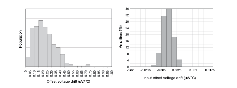
Upon recognizing this limitation and performing extensive experiments with different materials, TI identified a material combination that enabled the production of the OPA2182 with a maximum of only 12 nV/°C of offset drift across the full temperature range of -40°C to +125°C. Figure 2 compares the offset drift of the OPA2182 with a nonchopper amplifier, the OPA2140.

Figure 2: OPA2182 offset drift vs. OPA2140 laser-trimmed offset drift
Challenge No. 2: improving signal settling time
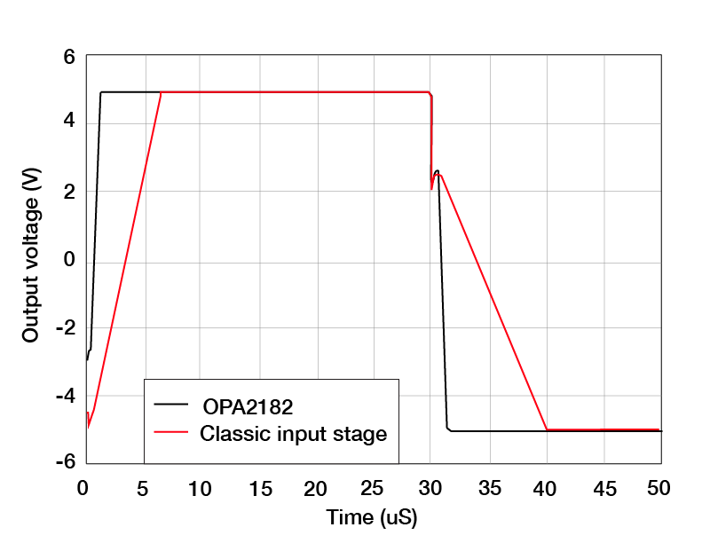
Another challenge when designing a precision signal chain is how to quickly and accurately settle the signal at the input of the ADC. Settling is particularly difficult for systems that use a multiplexer at the input to the signal chain to save both board space and system cost. The issue that arises with a switched input is that when the multiplexer switches channels, the ADC driver may see a step input. Many amplifiers have anti-parallel diodes connected between them for protection. When subjected to a step response, the inputs will no longer be approximately equal (as they are under normal operation), and one of the anti-parallel diodes will become forward-biased, drawing current from one input to the other. This current will flow through the multiplexer and the signal source, causing a delayed settling response.
To improve the settling time of the amplifier, TI added multiplexer (MUX)-friendly inputs to devices such as the OPA2182. This patented structure removes the anti-parallel diodes and enables the amplifier to settle a step input faster, as there is no erroneous current flowing through the signal source and multiplexer. Figure 3 compares the settling time of MUX-friendly inputs with a classic input stage.

Figure 3: Settling time of the OPA2182: a MUX-friendly input vs. a classic input stage
Although many challenges exist when designing a precision signal chain, chopper amplifiers like the OPA2182 can help simplify your designs, thanks to their improved offset drift performance and MUX-friendly inputs.


