Other Parts Discussed in Post: THP210 Differential signaling is becoming more popular in analog front ends, especially in factory automation designs, to interface with differential analog-to-digital converters (ADCs). In this article, I’ll discuss the advantages of a fully differential signal path, explain why precision is important and discuss how new fully differential amplifiers can meet precision challenges.
What is a fully differential amplifier?
A fully differential amplifier is a flexible device designed to provide a purely differential output signal centered at the user-configurable common-mode voltage. With this feature, the amplifier can control the output common-mode voltage independently from the differential voltage. The common-mode voltage is usually matched to the input common-mode voltage required by the ADC.

Increase the precision of your ADC driver.

Advantages of fully differential amplifiers
Differential signaling is becoming more popular in analog front ends. Factory automation is a segment where differential ADCs are popular. As such, a low-noise fully differential amplifier provides the necessary noise immunity and increases the dynamic range.
A differential signal has several advantages over its single-ended counterpart, including:
- Improved voltage swing. Both signals are out of phase, and the dynamic range is two times more than a single-ended output with the same voltage swing.
- Noise immunity. Since a differential signal is the difference of two single-ended signals that are out of phase to each other, any common-mode disturbance, power-supply noise, ground disturbance or electromagnetic interference will affect both signals equally – and ideally cancel each other out.
- Reduced harmonic distortion. Theoretical analysis of the distortion products of the differential output signal results in an even-order term cancellation. In reality, the distortion is also strongly dependent on the board layout and measurement setup.
Why is precision important?
Fully differential amplifiers typically drive high-resolution ADCs. The differential signal processing suppresses common mode, supply and ground disturbances. However, the offset, gain error and temperature drift of the preamplifier circuit can limit overall signal-chain accuracy.
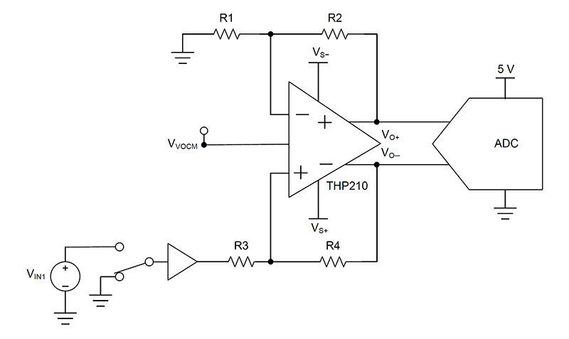
You can cancel out the offset error voltage by applying a few calibration schemes. Figure 1 shows a simplified circuit that you can use for offset calibration in differential input applications. The inputs are shorted to ground and provide an accurate 0-V signal. The offset error can directly be read at the output of the amplifier at the downstream ADC and further post-processed via software on a microcontroller. You can learn more about this technique in the TI Precision Labs video, “Understanding and Calibrating the Offset and Gain for ADC Systems.”

Figure 1: Offset calibration for differential signals
If the system allows, there are also ways to calibrate out the gain error. In order to minimize cost and complexity, many systems use one-point calibrations.
Gain and offset errors are common error sources that calibration techniques can cancel out by using calibration techniques. However, temperature drifts of the amplifier are sources that can dominate but are difficult or impossible to calibrate out. Temperature degradation is crucial for reliable measurements to improve the longevity of the equipment.
System designers often ask how to minimize these types of errors. The answer is simply to use devices with low drift specifications, such as the THP210 fully differential amplifier.
Let’s analyze the resulting drift error of a fully differential amplifier circuit. The main factors to consider when determining the error voltage over temperature are the:
- Input offset voltage drift: VIO vs. temperature = 0.35 μV/°C.
- Input bias current drift: IB vs. temperature = 15 pA/°C.
- Input offset current drift: IOS vs. temperature = 10 pA/°C.
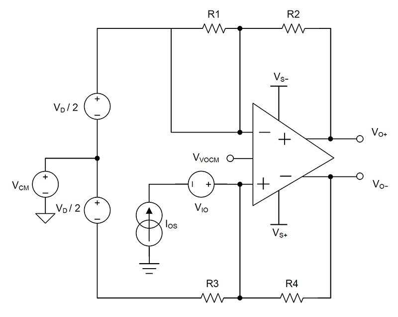
Figure 2 shows a fully differential amplifier configuration at a gain of 5 V/V with a feedback resistor network of 5 kΩ for R2/R4 and 1 kΩ for R1/R3, respectively. Both have tolerance of 0.1%.

Figure 2: Error model of a fully differential amplifier
Equation 1 calculates the total voltage error over a temperature range from 25°C to 125°C:

This error voltage is naturally reflected on the output of the application.
Given the maximum values of the THP210, the total drift error ends up at 36 μV, an improvement that’s four times greater than precision fully differential amplifiers currently available.
Conclusion
Differential signaling applications provide clear advantages over single-ended signals in many systems. Advantages include an improved voltage swing, better noise immunity, better common-mode rejection properties and low harmonic distortion.
To achieve high accuracy for the differential amplifier circuit, my recommendations are to carefully consider both the selection of the external resistor network and the temperature degradation effects of the amplifier.


