Other Parts Discussed in Post: BUF802 To reliably capture high-frequency signals and fast transient pulses, wide-bandwidth data acquisition systems like oscilloscopes and active probes require high-performance analog front-end (AFE) signal chains that must be able to:
- Support 1 VPP signals (at least) to ensure a high signal-to-noise ratio.
- Support DC to 500 MHz of high input-impedance (Hi-Z) to prevent loading of the device under test.
- Offer low noise and distortion to maintain high signal fidelity.
- Deliver high DC precision.
One way to overcome these design challenges is to create a composite loop-based approach that interleaves the low- and high-frequency signal chain in order to get DC precision and a wide large signal bandwidth.

Achieve ASIC-level performance with the BUF802

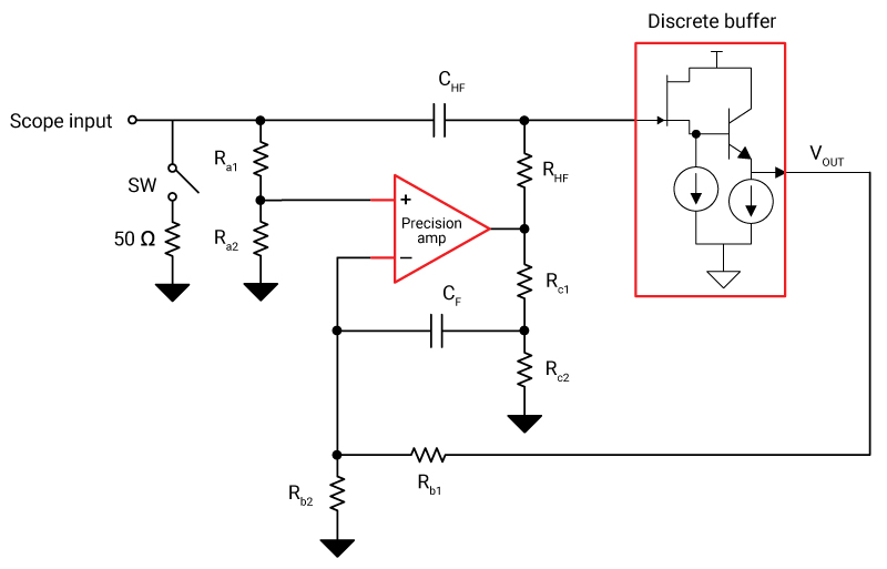
Given the complexity of implementing a composite loop-based circuit that meets system requirements, engineers usually have to either design custom application-specific integrated circuits (ASICs) or use multiple discrete components, as shown in Figure 1. Both options have drawbacks, including the need for specialized expertise with ASICs and additional design complexity. The two approaches also have trade-offs in terms of performance and cost: discrete implementations are less expensive than ASICs but cannot match their level of performance.

Figure 1: Discrete buffer composite loop with a precision amplifier AFE
In this article, I’ll explore the design challenges of discrete buffer composite loop implementations versus a single-chip implementation with the BUF802 Hi-Z buffer.
A discrete buffer composite loop architecture
The discrete implementation of the Hi-Z AFE in Figure 1 uses a precision amplifier and a discrete junction field-effect transistor (JFET)-based source follower circuit configured in a composite loop. The loop splits the input signal into low- and high-frequency components, taking both components to the output through two different circuits (transfer functions) and recombining them to reproduce a net output signal, as shown in Figure 2.

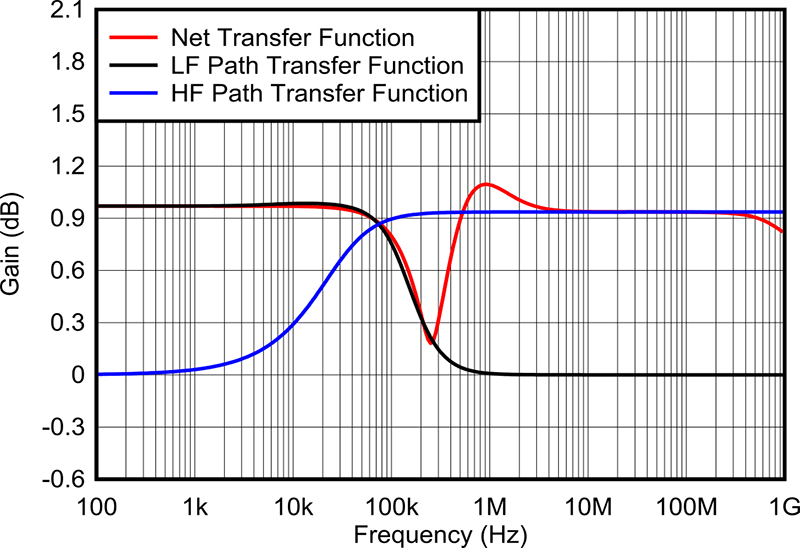
Figure 2: Discrete composite loop low- and high-frequency paths
The low-frequency path gives the net transfer function good DC precision, whereas the JFET source follower-based high-frequency path enables the net transfer function to have a wide large signal bandwidth, as well as low noise and distortion. One of the main challenges with the circuit shown in Figure 2 is achieving smooth interleaving of the two paths to ensure a flat frequency response. Any mismatch in the transfer function of the two paths will lead to discontinuity in the net transfer function frequency response resulting in a loss of signal fidelity.
The goal of a composite loop architecture
At DC or low frequencies, CHF (high-frequency capacitor) is open and the voltage output (VOUT) is controlled by the precision amplifier in the low-frequency path. The ratio of the alpha and beta resistor network controls the DC or low-frequency gain.
At high frequencies, CHF short circuits, and the precision amplifier runs out of bandwidth given the limited gain- bandwidth product. The discrete buffer operates as a JFET source and a negative-positive-negative emitter follower determines VOUT. The discrete buffer stage, referred to as gain (G) in Figure 3, determines the high-frequency path gain.

Figure 3: Discrete buffer composite loop architecture
At mid-frequencies, since both the low- and high-frequency paths determine the output, careful tuning of individual gain and interaction of poles and zeros is important to ensure a flat frequency response. Gain equalization at mid-frequencies is challenging to implement since the same components, CHF and RHF (high-frequency resistor) determine the poles of the low- and high frequency paths, as shown in figure 4.

Figure 4: Discrete buffer frequency response
The composite loop should have a flat frequency response and a high crossover frequency region in order to achieve low 1/f noise and fast overdrive recovery.
The complexities of a discrete implementation
Given the interdependency of the low- and high-frequency paths, as shown in Figure 5, the values of CHF and CF (compensation capacitor) are in tens of nanofarads in order to achieve a flat frequency response. But these values cause a crossover frequency range of tens to hundreds of hertz, which can limit the DC noise performance of the signal chain.

Figure 5: Interdependency of the low- and high-frequency paths
Another challenge when implementing the composite loop discretely is that the pole from the precision amplifier’s open-loop gain and the pole from the resistor-capacitor network of RHF and CHF contributes to the two-pole network in the low-frequency path, resulting in instability. The implementation of an additional network across the precision amplifier (labeled the gamma network in Figure 3) will compensate for that instability, but will require tuning in order to achieve a flatter frequency response, further adding to the complexity of creating a smooth frequency response across the operating range.
Implementing a composite loop with the BUF802
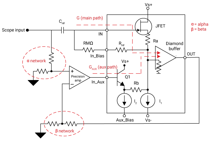
Since one of the major limitations of implementing a discrete composite loop is the interdependency between the low- and high-frequency paths and the need for an additional gamma network for compensation, the BUF802 has an auxiliary path internal to the device. Connecting the output of the precision amplifier to the auxiliary path creates a composite loop while ensuring isolation between the low- and high-frequency paths. Isolating the different frequency paths creates a higher crossover frequency region and eliminates the gamma network and compensation circuitry. The low- and high-frequency signal components recombine inside the BUF802 and are reproduced at the OUT pin, as shown in Figure 6.

Figure 6: Composite loop precision amplifier with an internal BUF802
Conclusion
An integrated Hi-Z buffer such as the BUF802 helps solve the complex challenges of a composite loop-based implementations. The BUF802’s integrated protection features like input/output clamps help protect subsequent stages in the signal chain, reduce overdrive recovery time and input capacitance, and increase system reliability.
When considering an AFE for today’s applications, you must also keep in mind future measurement needs, which usually require additional bandwidth. This bandwidth can go a long way in both measurement accuracy and ensuring system design investments stay relevant for future test requirements.
Additional resources


