(This is a guest technical article from Cadence? Design Systems.)
Part 1 of this series discussed optimizing your simulation profile in PSpice? for TI. After creating a schematic and a simulation profile, you are ready to simulate your circuit design and view the results.
The results must be accurate, of course. However, the effectiveness of a simulation is only half as good as the flexibility and ease of viewing the results. In that context, you can explore “markers” – objects that you place on points in your circuits to mark them so that you can view the corresponding waveforms at those points. In this article, we will walk through how to take advantage of markers in your simulation.
Markers have two advantages: flexibility and a reduction in data file size. You can add markers at any time before or after running a simulation, making it a flexible way to view results. To reduce the data file size, you can set up PSpice for TI to save results only for marked wires and pins. By default, PSpice for TI stores all net voltages and device currents for each step, such as time or frequency points. To reduce data size, you must select the At Markers Only option in the Data Collection Settings tab of the Simulation Settings dialog box before you run the simulation. (For more information on the settings simulations, see Part 1 of this series.)
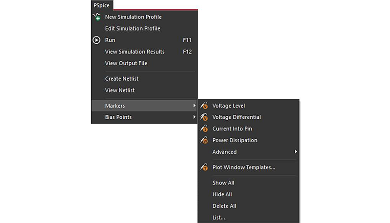
To place markers, choose the marker type you want by selecting PSpice – Markers, as shown in Figure 1. Then, click the point where you want to place the marker.
Markers and their types
The PSpice – Markers menu shown in Figure 1 has options for various marker types. Use one or more types of markers based on the results you want to see.

Figure 1: PSpice – Markers options
You can also use the buttons from the toolbar on top-right of the application, as shown in Figure 2.

Figure 2: Toolbar buttons for markers
Table 1 lists the expected results and their corresponding marker types. Advanced markers are active only for AC sweep/noise analysis, as you will see in the next section.
|
Waveform/result expected
|
Marker type
|
|
Analog voltage
|
Voltage Level
|
|
Digital value (high or low)
|
Voltage Level
|
|
Voltage differential between any two nodes
|
Voltage Differential
|
|
Current
|
Current Into Pin
|
|
Power
|
Power Dissipation
|
|
Under the Advanced menu:
|
|
Decibel (20log10)
|
dB Magnitude of Voltage
dB Magnitude of Current
|
|
Phase
|
Phase of Voltage
Phase of Current
|
|
Group delay
|
Group Delay of Voltage
Group Delay of Current
|
|
Real part
|
Real Part of Voltage
Real Part of Current
|
|
Imaginary part
|
Imaginary Part of Voltage
Imaginary Part of Current
|
Table 1: Waveform results and corresponding marker types
A future installment of this series will cover template markers available within the Markers menu (the Plot Window Templates option).
Placing markers and viewing results
When you run a simulation for the first time without any markers defined, PSpice for TI displays a blank screen without any waveforms. If you want to see the results, you either add markers or traces. This article discusses only markers, but a future installment of this series will cover traces.
As mentioned earlier, you can add markers before or after running a simulation. In this example, you will add a marker after running a simulation, but the steps for adding markers before running a simulation are identical.
To simulate a design and then add a voltage marker, follow these steps:
- Choose PSpice – Run to run the simulation. PSpice opens after the simulation is complete, but you will not see any waveforms because you have not yet added any markers.
- Choose PSpice – Markers – Voltage Level. The Voltage-level probe sticks to the cursor, as shown in Figure 3.
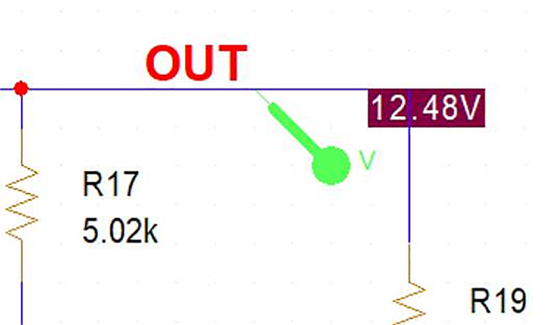
- Click at the point where you want to see the result, which in this example is the OUT node shown in Figure 4.

Figure 3: Voltage-level probe

Figure 4: Marker placed on the OUT node
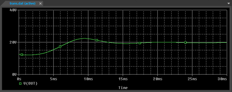
PSpice for TI displays the simulation result you are interested in, as shown in Figure 5.

Figure 5: Simulation results for the marker placed on the OUT node
You can then add any other marker according to your needs. For example, if you wanted to see the output voltage level at a node in decibels, you could add the dB Magnitude of Voltage advanced marker at that node.
To add a dB Magnitude of Voltage advanced marker, follow these steps:
- Because you are adding an advanced marker, confirm that you are running the simulation for AC Sweep/Noise Analysis type.
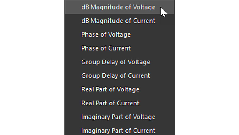
- Choose PSpice – Marker – Advanced – dB Magnitude of Voltage. Figure 6 shows the Advanced submenu options.
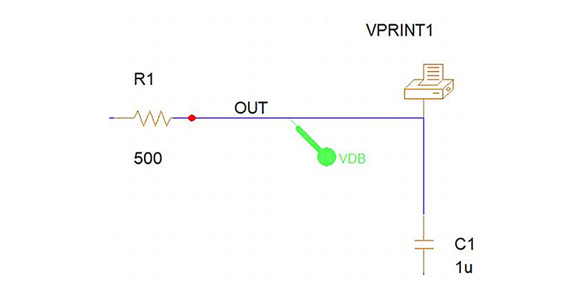
- Click at the point you want to see the result. Figure 7 shows a dB Magnitude of Voltage marker (abbreviated as VDB) placed at the OUT node.

Figure 6: Advanced submenu options

Figure 7: VDB at the OUT node
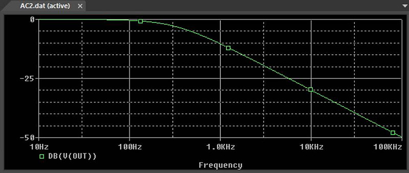
PSpice now shows the output voltage level in decibels at the OUT node, as shown in Figure 8.

Figure 8: Voltage level in decibels at the OUT node
Conclusion
Now that you know how to select the markers you need, you can use them in your schematics and take advantage of their flexibility. To get started, download PSpice for TI today.
Read more in this series


